Si5367, Figure 12. si5367 clock multiplier block diagram, Si53xx-rm – Silicon Laboratories SI5375 User Manual
Page 27: Rev. 1.2 27
Si53xx-RM
Rev. 1.2
27
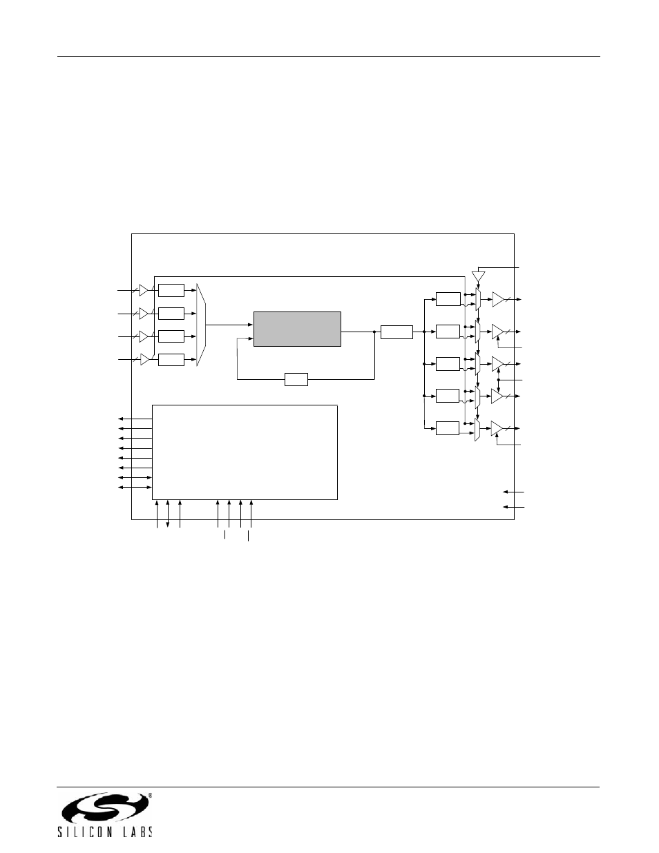
3.12. Si5367
The Si5367 is a low jitter, precision clock multiplier for applications requiring clock multiplication without jitter
attenuation. The Si5367 accepts four clock inputs ranging from 10 to 707 MHz and generates five frequency-
multiplied clock outputs ranging from 2 kHz to 945 MHz and select frequencies to 1.4 GHz. The Si5367 input clock
frequency and clock multiplication ratio are programmable through an I
2
C or SPI interface. The DSPLL loop
bandwidth is digitally programmable from 150 kHz to 1.3 MHz. Operating from a single 1.8, 2.5, or 3.3 V supply, the
Si5367 is ideal for providing clock multiplication in high performance timing applications. See "6. Microprocessor
Controlled Parts (Si5319, Si5324, Si5325, Si5326, Si5327, Si5328, Si5367, Si5368, Si5369, Si5374, Si5375, and
Si5376)" on page 63 for a complete description.
Figure 12. Si5367 Clock Multiplier Block Diagram
Note: Not recommended for new designs. For alternatives, see the Si53xx family of products.
C2A
CS0_C3A
C2B
CS1_C4A
INT_ALM
C1A
CKIN_1+
CKIN_1–
CKIN_2+
CKIN_2–
C3B
CKIN_3+
CKIN_3–
CKIN_4+
CKIN_4–
C1B
VDD
GND
CKOUT_1+
CKOUT_1–
÷ NC1
1
0
CKOUT_2+
CKOUT_2–
÷ NC2
1
0
CKOUT_3+
CKOUT_3–
÷ NC3
1
0
CKOUT_4+
CKOUT_4–
÷ NC4
1
0
2
2
2
2
2
2
2
2
f
OSC
f
3
DSBL2/BYPASS
DSBL34
DSBL5
SD
A
_
SD
O
SCL
SDI
A[
1:0]
RS
T
CM
ODE
BYPASS/DSBL2
Control
÷ N3_2
÷ N3_1
÷ N2
3
÷ N3_3
÷ N3_4
CKOUT_5+
CKOUT_5–
÷ NC5
1
0
2
A[
2]
/S
S
÷ N1_HS
DSPLL
®