Si5328, S i 5 3 x x - r m – Silicon Laboratories SI5375 User Manual
Page 24
S i 5 3 x x - R M
24
Rev. 1.2
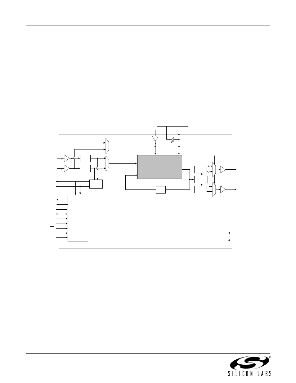
3.9. Si5328
The Si5328 is a jitter-attenuating precision clock multiplier for applications requiring sub-1 ps jitter performance and
digitally-programmable ultra-low-loop BW ranging from 0.05 to 6 Hz. When combined with a low-wander, low-jitter
reference oscillator, the Si5328 meets all of the wander, MTIE, TDEV, and other requirements that are listed in ITU-
T G.8262. The Si5328 accepts two input clocks ranging from 8 kHz to 346 MHz and generates two output clocks
ranging from 2 kHz to 346 MHz. The device provides virtually any frequency translation combination across the
operating range. The Si5328 input clock frequency and clock multiplication ratio are programmable through and
I
2
C or SPI interface. Operating from a single 1.8, 2.5, or 3.3 V supply, the Si5328 is ideal for providing multiplication
and jitter/wander attenuation in high-performance timing applications like SyncE timing cards. See "6.
Microprocessor Controlled Parts (Si5319, Si5324, Si5325, Si5326, Si5327, Si5328, Si5367, Si5368, Si5369,
Si5374, Si5375, and Si5376)" on page 63 for a complete description. Also see “AN775: Si5328 ITU-T G.8261
SyncE Compliance Test Report" and “AN776: Using the Si5328 in a G.8262 Compliant SyncE Application".
Figure 9. Si5328 Clock Multiplier and Jitter Attenuator Block Diagram
÷ N31
INT_C1B
÷ NC1
÷ NC2
Signal
Detect
VDD
GND
C2B
0
1
f
3
CKOUT_2 +
CKOUT_2 –
CKOUT_1 +
CKOUT_1 –
/
/
2
2
1
0
1
0
f
OSC
RATE[1:0]
CS_CA
RST
Control
XA
XB
CKIN_1 +
CKIN_1 –
2
2
CKIN_2 +
CKIN_2 –
÷ N32
0
1
3
BYPASS
÷ N2
DSPLL
÷ N1_HS
DSPLL
®
TCXO or Refclock
A[1:0]
A[2]/SS
SDI
SCL
SDA_SDO
CMODE
LOL