Si5325, Si53xx-rm – Silicon Laboratories SI5375 User Manual
Page 21
Si53xx-RM
Rev. 1.2
21
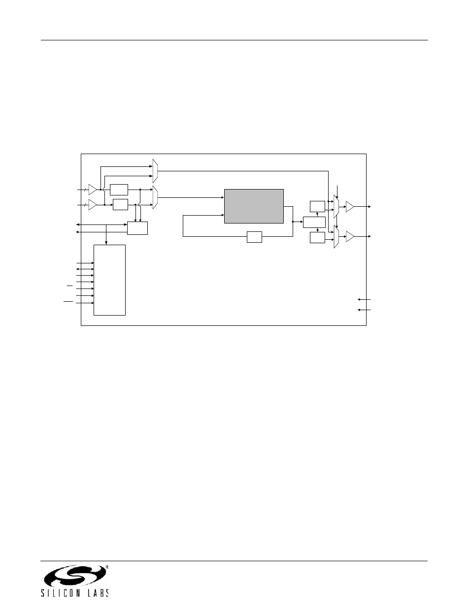
3.6. Si5325
The Si5325 is a low jitter, precision clock multiplier for applications requiring clock multiplication without jitter
attenuation. The Si5325 accepts dual clock inputs ranging from 10 to 710 MHz and generates two independent,
synchronous clock outputs ranging from 2 kHz to 945 MHz and select frequencies to 1.4 GHz. The Si5325 input
clock frequency and clock multiplication ratios are programmable through an I
2
C or SPI interface. The DSPLL loop
bandwidth is digitally programmable from 150 kHz to 1.3 MHz. Operating from a single 1.8, 2.5, or 3.3 V supply, the
Si5325 is ideal for providing clock multiplication in high performance timing applications. See "6. Microprocessor
Controlled Parts (Si5319, Si5324, Si5325, Si5326, Si5327, Si5328, Si5367, Si5368, Si5369, Si5374, Si5375, and
Si5376)" on page 63 for a complete description.
Figure 6. Si5325 Low Jitter Clock Multiplier Block Diagram
Note: Not recommended for new designs. For alternatives, see the Si533x family of products.
÷ N31
INT_C1B
÷ NC1
÷ NC2
Signal
Detect
C2B
0
1
CKOUT_2 +
CKOUT_2 –
CKOUT_1 +
CKOUT_1 –
/
/
2
2
1
0
1
0
SDA_SDO
RST
SCL
Control
SDI
A[2]/SS
A[1:0]
CMODE
CKIN_1 +
CKIN_1 –
2
2
CKIN_2 +
CKIN_2 –
÷ N32
0
1
BYPASS
÷ N2
f
3
DSPLL
®
VDD
GND
÷ N1_HS
f
OSC