Timing characteristics – Seiko Instruments G1216B1N000-3D0E User Manual
Page 18

AN.No.G1216B1N000-3D0E
- 15 -
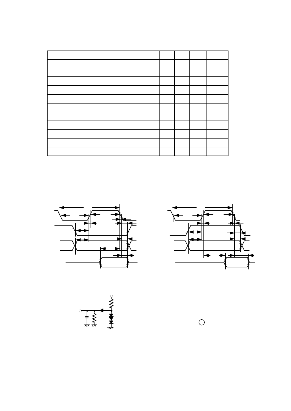
3.2 Timing Characteristics
t
f
t
CYC
t
CYC
R / W
2.4V
0.4V
t
DDR
t
DHR
t
AH
t
AH
2.0V
0.8V
t
AS
t
AS
2.0V
0.8V
t
DHW
t
DSW
t
AS
t
AS
2.0V
0.8V
t
AH
t
AH
t
r
2.0V
0.8V
P
WEL
2.0V
0.8V
P
WEH
D
1
Test point
C
R
R
L
D
2
D
3
D
4
25
25
320
1000
450
450
140
10
200
10
20
t
CYC
P
WEH
P
WEL
t
r
t
f
t
AS
t
AH
t
DSW
t
DDR
t
DHW
t
DHR
ns
ns
ns
ns
ns
ns
ns
ns
ns
ns
ns
1, 2
1, 2
1, 2
1, 2
1, 2
1, 2
1, 2
1
2, 3
1
2
E cycle time
E pulse width (H)
E pulse width (L)
E rise time
E fall time
Address setup time
Address hold time
Data setup time
Data delay time
Data hold time during write
Data hold time during read
Note
unit
Max.
Typ.
Min.
Symbol
Item
Note 1:
When the MPU writes:
Note 3: Load circuits (DB
0
to DB
7
)
E
t
f
t
r
P
WEL
2.0V
0.8V
P
WEH
Note 2:
When the MPU reads:
DB
0
to DB
7
R
L
= 2.4 k
R
= 11 k
C
= 130 pF (including jig capacity)
Diodes D1 to D4 are 1S2074 H .
E
DB
0
to DB
7
R / W
CS1, CS2
D/I
CS1, CS2
D/I
2.0V
0.8V
