Ic block diagrams, Ic pin function description, Str-de375 – Sony Ericsson SONY STR-DE375 User Manual
Page 18
18
18
STR-DE375
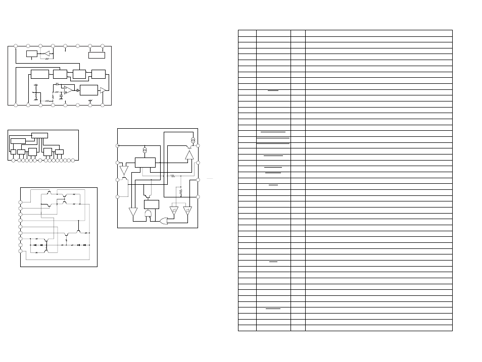
3-11. IC BLOCK DIAGRAMS
3-12. IC PIN FUNCTION DESCRIPTION
IC103
µPD780206GF-092-3BA (DISPLAY BOARD)
Pin No.
1
2
3
4
5
6
7
8
9
10
11
12
13
14
15
16
17
18
19
20
21
22
23
24
25
26
27
28
29
30
31
32
33
34
35
36
37
38
39
40
41
42
43
44
45
46
47
48
49
50
I/O
I
O
O
O
—
—
O
O
O
I
—
—
—
—
I
—
O
O
O
O
I
O
I
I
—
I
—
I
I
I
I
I
I
—
—
—
—
I
I
—
—
—
—
—
O
—
I
O
I
I
Description
Power supply to
µ-com
Control Video IC switching (Not used)
Control Video IC switching (Not used)
Control mute of Video IC (Not used)
Not used
Not used
Volume IC data
Volume IC clock
Volume IC enable
Read
µ-com reset signal
Connection to a crystal resonator
Connection to a crystal resonator
Programming pow. supply (Cnnected to ground)
Not used
Read decoded RDS data
Power supply to
µ-com
Chip enable for ICs
Output clock signal
Output data signal
Chip enable for ICs
Tuner has tuned to a freq.
Muting tuner during scanning
Tuned freq. has stereo
Input tuner freq. data
Analog ground
Read remote sensor signal
Not used
Detect RDS signal level
Read version setting
Read key push signal
Read key push signal
Read key push signal
Read key push signal
Analog Power Supply
Analog reference voltage
Not used
Not used
Read decoded RDS clock
Read signal when AC off
µ-com ground
Not used
Not used
Not used
Not used
Control MUTING LED
Power supply to
µ-com
Detect Protector Status
Control Power relay
Read volume encoder changing
Read volume encoder changing
Pin Name
VDD +5V
S1
S2
IC.MUTE
P34
P33
S.DATA (M61501FP)
S.CLK (M61501FP)
S.CE (M61501FP)
RESET
X2
X1
VSS
—
RDS.DATA.IN
VDD +5V
S.CE (LV1050M)
S.CLK(DOLBY.TUNER)
S.DATA(DOLBY.TUNER)
S.CE (TUNER)
AUTO-STOP
T.MUTE
STEREO-IN
PLL.DATA
AVSS
SIRCS
P16
SIGNAL
VERSION
A/D IV
A/D III
A/D II
A/D I
AVDD +5.0V
AVREF
P03
P02
RDS.CLK.IN
STOP
VSS
P74
P73
P72
P71
MUTING LED
VDD +5.0V
PROTECT
POWER-RY
ENCODER
ENCODER
IC701, IC702 uPC2581V (MAIN BOARD)
PROTECTOR
DRIVE
1
2
3
4
5
6
7
8
9 10 11 12 13 14 15
PRE
DRIVE
PRE
DRIVE
BIAS CIRCUIT
REG
MUTE
+VOUT1
–
VOUT1
COMP1
NF1
IN1
GND
IN2
NF2
COMP2
–
VOUT2
+VOUT2
VCC1
VCC2
VEE
DRIVE