Multiburst, Dma support, Figure 5: multiburst operation – M-Systems Flash Disk Pioneers Flash Memory User Manual
Page 12: Internal data transfers, External data transfers
Implementing MLC NAND Flash for Cost-Effective, High-Capacity Memory
91-SR-014-02-8L
12
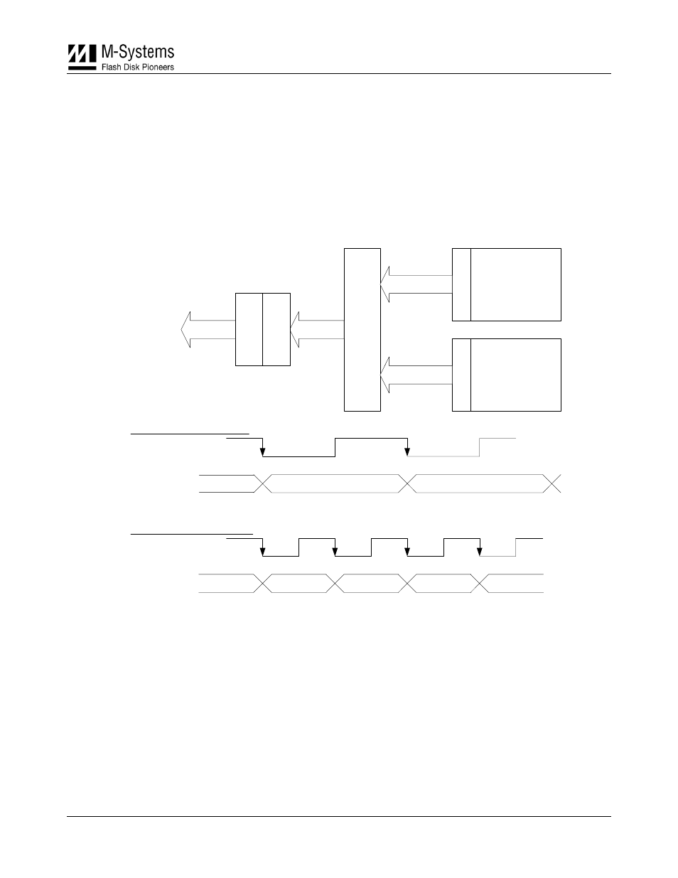
MultiBurst
To improve MLC read performance rates, x2 technology incorporates a feature called MultiBurst.
MultiBurst enables parallel read access from two 16-bit planes to the flash controller, thereby
achieving the desired output data rate for the host. The host accesses the first word of a page with a
relatively slow access time, but each subsequent word with a very fast access time. Two cycles of 16
bits each are sent to the host at a clock rate set by the host rather than limited by flash operation, as
shown in Figure 5.
Flash Plane
W
O
R
D
0
Flash Plane
W
O
R
D
1
32-bi
t Dat
a
M
ux
16-bit to
Host
16-bit Data
16-bit Data
WO
RD
0
WO
RD
1
FIFO
32-bit Transfer
32-bit Transfer
Data transfer from
Flash Planes to FIFO
/Flash_OE
Internal data transfers
16-bit Transfer
16-bit Transfer
16-bit Transfer
16-bit Transfer
/DiskOnChip_OE
Data transfer from
FIFO to Host
External data transfers
Figure 5: MultiBurst Operation
DMA Support
By enabling DMA operation, x2 technology reduces the CPU overhead. This is a particularly useful
feature for transferring large files in support of Real-Time Operating Systems (RTOS). In addition, it
can be used to enhance overall system performance by reducing boot time. In this case, the DMA
mechanism is used to quickly transfer large blocks of code from the media into shadow RAM.
When comparing Mobile DiskOnChip G3 to raw flash products, such as Intel StrataFlash or AMD
MirrorBit, this capability has at least a threefold benefit: increased performance, easier integration,
and reduced external part count by allowing direct connection to a DMA controller without
additional hardware.