Applications information, Pin configuration chip information, Table 1. output clamp level – Rainbow Electronics MAX7446 User Manual
Page 5
Filter
Filter Response
The reconstruction filter consists of two 2nd-order Sallen-
Key stages. The Butterworth-type response features a
maximally flat passband for NTSC and PAL bandwidths.
The stopband offers at least 43dB (typ) of attenuation at
a video-encoder DAC sampling frequency of 27MHz
(see the Typical Operating Characteristics).
High-Frequency Boost
The +1.2dB high-frequency boost on channel A increas-
es image sharpness by compensating for signal degra-
dation and roll-off in the video encoder. Channels B, C,
and D (RGB) do not boost high-frequency signals and
have a flat response over the video bandwidth.
Output Buffers
Each output buffer has a fixed gain of +6dB and can
drive two 150
Ω video loads with a 2V
P-P
signal. The
MAX7446 can drive an AC load or drive the video load
directly without using a large output capacitor. The out-
put buffers drive DC loads with an output blanking level
of less than 1V.
Output Clamp Level
When a sync pulse is detected on channel A, the DC
restore loop is activated. The function of the loop is to
set the DC value of the video signal to a specified volt-
age. See Table 1 for clamp levels.
Applications Information
Input Considerations
Use 0.1µF ceramic capacitors to AC-couple the inputs.
These input capacitors store a DC level so the outputs
are clamped to an appropriate DC voltage level.
Output Considerations
The outputs are typically connected to a 75
Ω series
back-match resistor followed by the video cable.
Because of the inherent divide-by-two of this configura-
tion, the voltage on the video cable is always less than
1V, complying with industry-standard video require-
ments such as the European SCART standard (which
allows up to 2V of DC on the video cable). The video
buffer can also drive an AC-coupled video load. Good
video performance is achieved with an output capacitor
as low as 220µF.
Power-Supply Bypassing and Layout
The MAX7446 operates from a single +5V supply.
Bypass V
CC
to GND with a 0.1µF capacitor. Place all
external components as close to the device as possible.
Exposed Pads
The TSSOP-EP package has an exposed pad on the
bottom of the package. This pad is electrically connect-
ed to GND and should be connected to the ground
plane for improved thermal conductivity. Do not route
signals under this package.
MAX7446
4-Channel Video Filter for RGB and CVBS Video
_______________________________________________________________________________________
5
14
13
12
11
10
9
8
1
2
3
4
5
6
7
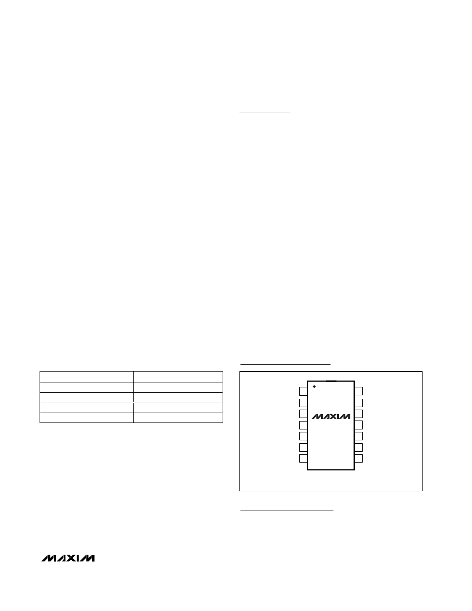
OUTA
OUTB
OUTC
OUTD
IND
INC
INB
INA
TOP VIEW
MAX7446
V
CC
GND
GND
GND
GND
DISABLE
TSSOP
Pin Configuration
Chip Information
TRANSISTOR COUNT: 6300
PROCESS: BiCMOS
Table 1. Output Clamp Level
CHANNEL
CLAMP LEVEL (V)
A
0.8
B
1.4
C
1.4
D
1.4