Circuit adjustments, 1.a board adjustment, 2.t1 board adjustment – Sony FDL-PT222 User Manual
Page 7
– 7 –
FDL-PT222
SECTION 3
CIRCUIT ADJUSTMENTS
3-1.A BOARD ADJUSTMENT
[+4.5V ALIGNMENT (RV601)]
Using a digital voltmeter measuring the voltage between
JL32 (+4.5V) and JL33 (GND). Adjust RV601 to obtain
the value shown below.
Standard Value = 4.45V
±
0.05VDC
S601 position = UHF position
[+30.0V CHECK]
Check the voltage across JL29 (+30.0V) and JL33 (GND) .
Standard Value = 30.5V
±
1.5VDC
[AUDIO OUTPUT CHECK]
1. Feed the audio signal 1kHz 100% modulated.
2. Set RV501 to maximum.
3. Connect an oscilloscope between JL23 (SP) and JL15 (SP
GND).
4. Check the waveform on the oscilloscope becomes the stan-
dard value.
Standard Value = 1.5V-2.8Vp-p
3-2.T1 BOARD ADJUSTMENT
[VIF.AFT COARSE ADJUSTMNT (T201, T202)]
[
SETUP
]
1. Set S601 on the A board to VHF position.
2. Apply no signal to JL18 (RF).
3. Connect a 1 k
Ω
resistor between JL77 (+4.5V) and
JL28 (RF AGC).
4. Apply a sweep signal across JL26 (IF) and JL27(IF GND).
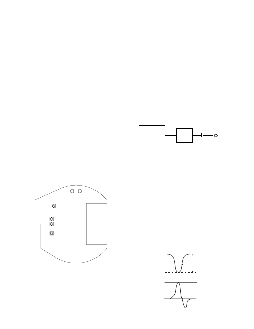
(Fig. 3-1)
Note
: Set the sweep signal for JL26 to -30
±
5dBm. Keep the
distance to the ATT output JL26 as short as possible.
Fig. 3-2
[ADJUSTMNT]
1. Connect an oscilloscope between JL72 (VIDEO) and JL71
(A.GND) and apply an external voltage (MGC) to JL26 to
obtain a waveform as shown in Fig. 3-2 (make sure not to
clip the extremely short portion).Adjust T202 so that the po-
sition at 45.75 MHz is the lowest point.
Note
: Align JL51 (MGC) external voltage for approximately
a 1.0 Vp-p. Make sure that the JL51 (MGC) external
voltage does not exceed 4.3VDC.
2. Remove the external voltage (MGC) from JL51.
3. Connect an oscilloscope between JL31 (AFT) and JL30
(D.GND) and make a coarse adjustment of T201 so that wave-
form is close to zero at the 45.75 MHz position.
4. Remove the 1 kilohm resistor connected between JL77 (+4.5V)
and JL28 (RF AGC).
Fig. 3-1
JL26
75
Ω
6dB
fo=45.75MHz
±
5kHz
SWEEP
MARKER
GENERATOR
0.01
µ
F
ATT
1Vp-p
45.75MHz
0
TU101
RV201
T201 T202
RV002
RV004
RV001
- T1 board - (Component side)