Samsung S3F80JB User Manual
Page 345

Important Note
S3F80JB
3
3. DIFFERENCE S3F80JB AND S3F80J9
3.1 WHEN TEST PIN = “1(VDD)”
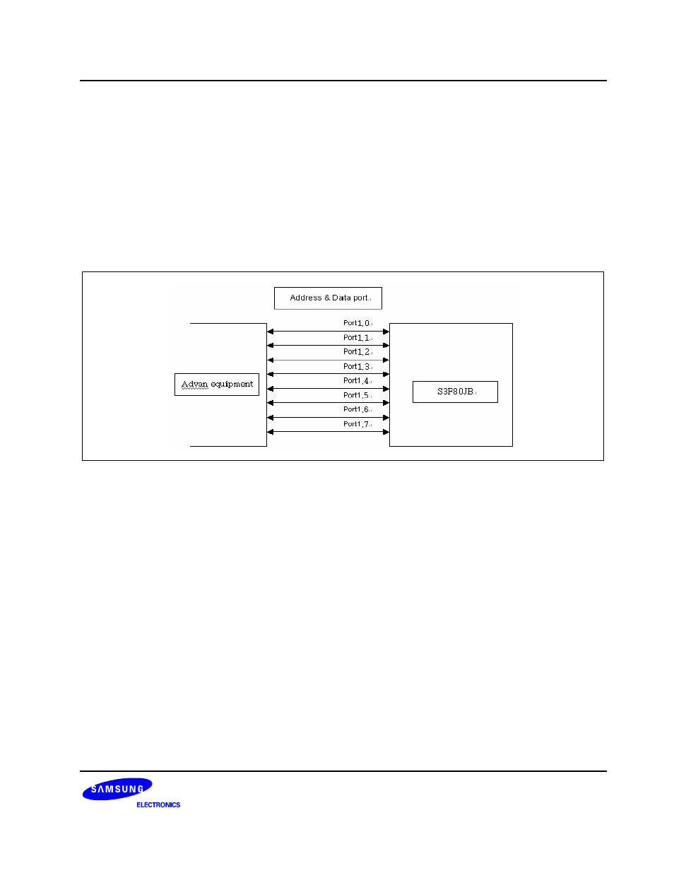
This is Fabrication Test mode (For Design team & PE ) : Design team & PE team tested S3F80JB by using
ADVAN equipment When testing S3F80JB, port1.0~1.7 is set to
address port and data port for chip test.
So, output disable signal of Port1.0~1.7 is toggling to Input/Output
mode.
¾ When S3F80JB
Port1.0~1.7 is used to address & data port between Advan equipment and S3F80JB. When Advan equipment
sends data to S3F80JB, port1.0~1.7 is input mode. And when Advan equipment receives next address to
S3F80JB, port1.0~1.7 is output mode. I.e, port1.0~1.7 is toggling to Input/Output mode during chip test.
