6 floppy disk connector: floppy – Intel SYS7180VE User Manual
Page 12
CHAPTER 2 –Hardware Installations
SYS7180VE
User’s Manual
17
These connectors support the provided IDE hard disk ribbon cable. After
connecting the single end to the board, connect the two plugs at the other end to your hard
disk(s). If you install two hard disks, you must configure the second drive to Slave mode
by setting its jumper accordingly. Please refer to your hard disk documentation for the
jumper setting.
Pin Description Pin Description Pin Description
1
Reset #
2
GND
3
Data 7
4
Data 8
5
Data 6
6
Data 9
7
Data 5
8
Data 10
9
Data 4
10 Data 11
11 Data 3
12 Data 12
13 Data 2
14 Data 13
15 Data 1
16 Data 14
17 Data 0
18 Data 15
19 GND
20 No connector
21 No connector
22 GND
23 IOW #
24 GND
25 IOR #
26 GND
27 IOCHRDY
28 No connector
29 No connector
30 GND-Default
31 Interrupt
32 No connector
33 SA1
34 No connector
35 SA0
36 SA2
37 HDC CS0 #
38 HDC CSI #
39 HDD Active #
40 GND
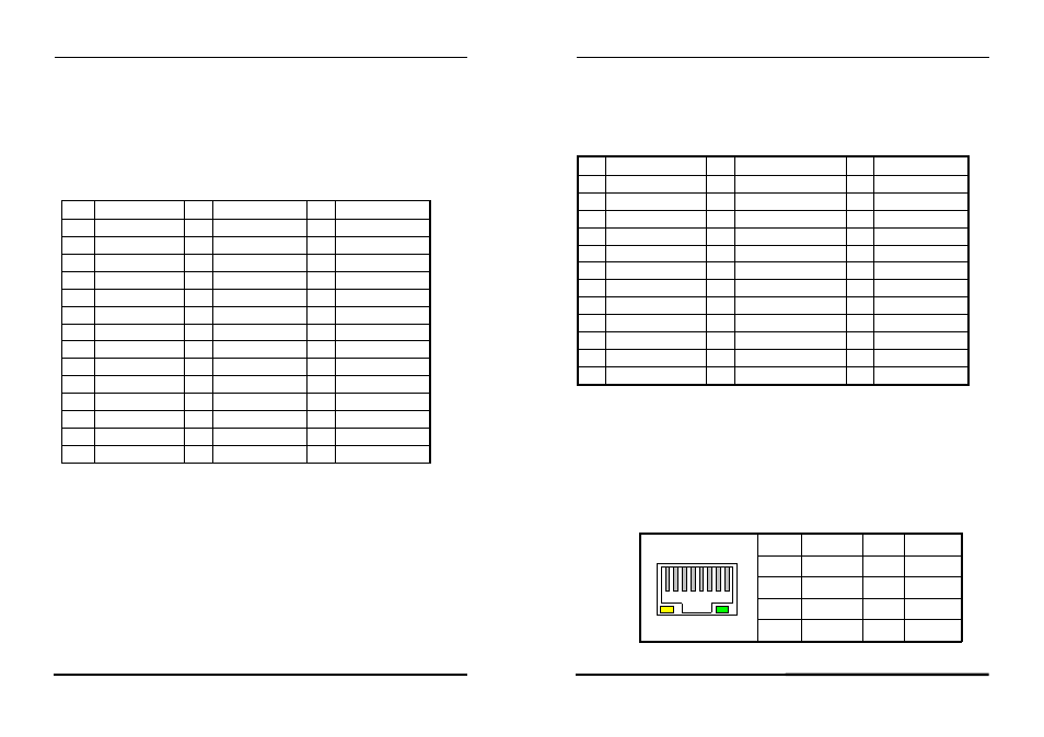
2.5.6 Floppy Disk Connector: FLOPPY
The floppy interface can be configured for the following floppy drive capacities
and sizes:
360 KB, 5.25-inch
1.2 MB, 5.25-inch
720 KB, 3.5-inch
1.2 MB, 3.5-inch (driver required)
1.25/1.44 MB, 3.5-inch
CHAPTER 2 –Hardware Installations
18
SYS7180VE
User’s Manual
2.88 MB, 3.5-inch
This connector supports the provided floppy drive ribbon cable. After connecting
the single and to the board, connect the two plugs on the other end to the floppy drives.
Pin Description Pin Description Pin
Description
1
GND
2
Reduce write current
3
GND
4
No connector
5
GND
6
No connector
7
GND
8
Index#
9
GND
10
Motor enable A#
11
GND
12
Drive select B#
13
GND
14
Drive select A#
15
GND
16
Motor enable B#
17
GND
18
Direction#
19
GND
20
STEP#
21
GND
22
Write data#
23
GND
24
Write gate#
25
GND
26
Track 0 #
27
GND
28
Write protect#
29
GND
30
Read data#
31
GND
32
Side 1 select#
33
GND
34
Disk change#
2.5.7 Adapter connector for 10/100 LAN: LAN1
This connector is for the LAN adapter that has LED indicate the 10/100Mbps
transfer rate / Link / Act status of Ethernet capability of the CPU card. The follow table
shows the pin assignments of this connector.
PIN No.
Function
PIN No. Function
1 TX+ 5
GND
2 TX- 6 NC
3 NC 7
RX+
C N 1 3
1 2 3 4 5 6 7 8
L i n k T r a n s m i t
L E D L E D
4 GND 8 RX-