Drawn design check issues – MiTAC 7521 PLUS/N User Manual
Page 178
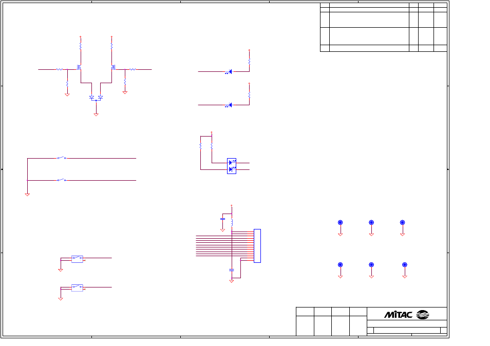
DRAWN
DESIGN CHECK
ISSUES
R00
DATE
R0A
ECR
05/26/2000
DESCRIPTION OF CHANGE
REV
07/04/2000
1.Relayout base on R00
2.Remove SW3 & SW4 pin 4
3.Remove 74164 blanking circuit
4.Reverse BATT_G# & BATT_R# pin assignment error
5.Change power source from VDD5 to VDD5S for LEDs
6.Remove the reserved circuit
R01
1.Relayout base on R0A
2.Change Batt LED from BRPG1201W to 19-22SRVGC/TR8
3.Change Batt LED RES to fix orange color
4.Change Mail LED from L-1384AD/1GD and
L-1384AD/1YD to L-59BL/1GYW
5.Remove one of VDD5S circuit
08/15/2000
R02
1.Relayout base on R01
09/20/2000
2.Add Q1,Q2 (2N7002) to enhance mail LED brightness
!
"
#$% &
'(
)
#*
+,+-./0
+'+-./0
0
0
1+23.'0
1+3'450
1+60
0
/.,,23+,67
+'+-./0
+,+-./0
0
1+23.'0
1+3'450
1+'0
1+60
1+'0
/.,,23+,67
6'..&+,67
6'..&+,67
6&
6&
6&
6&
6&
8
8
8
8
6&
6&
6&
6&
6&
6&
6&
6&
8
6&
8
3
984:1
;984:1
'
: -
9
'
: -
9
3
;11;
;11+
9
39
;11;
;11+
9
'
99
9
'
99
9
<6
9:42:
<6
9:42:
<6
9:42:4,
'
9
3
984:1
;984:1
9
,;6
1
-
=
5455;4:<<
9;;;
9
9
9
9
<69
9:42:4,
' 9
9
,;6
1
-
,;,46/3
>4&1
9
<6
<64: 42
,
.1
9
:>
8
9
<6
<64: 42
'9
9
'
'
'
99
9
D
S
&
6
D
S
&
6
VG
SR
; '864'
9