Chapter 3, Board layout – Lanner LEC-7106 User Manual
Page 15
15
Board Layout
Chapter 3
Embedded and Industrial Computing
Dual USB Port Connector #0 and #1 (USB1):
Dual USB Port Connector #2 and #3 (USB2)
USB Pin Header (USB3)
Reset Button (RST1)
Pin NO.
description
1
RsT_BTN
2
GNd
3
GNd
4
N/A
Power-on Switch through Phoenix Contact (J12): A
Phoenix connector for distant power switch.
Mini PCI Express Connector (for 3G/GPS card with USB
signal, MPCIE1):
PIN
Pin Name
PIN
Pin Name
1
WAKE#
2
VCC3.3
3
N/A
4
GNd
5
N/A
6
VCC1.5
7
CLKREQ#
8
VREG_UsIM
9
GNd
10
UIM_dATA
11
CLK_PCIE_MINI_
N1
12
UIM_CLK
13
CLK_PCIE_MINI_P1
14
UIM_REsET
15
GNd
16
UIM_VPP
17
RsV
18
GNd
19
RsV
20
RF_KILL_N1
21
GNd
22
PLTRsT
23
PCIE_RX_N2
24
PCIE1_P24
25
PCIE_RX_P2
26
GNd
27
GNd
28
VCC1.5
29
GNd
30
sMBCLK
31
PCIE_TX_N2
32
sMBdATA
33
PCIE_TX_P2
34
GNd
35
GNd
36
UsB_N6
37
GNd
38
UsB_P6
39
VCC3.3
40
GNd
41
VCC3.3
42
LEd1_WWAN
43
GNd
44
LEd1_WLAN
45
RsV
46
LEd1_WPAN
47
RsV
48
VCC1.5
49
RsV
50
GNd
51
RsV
52
VCC3.3
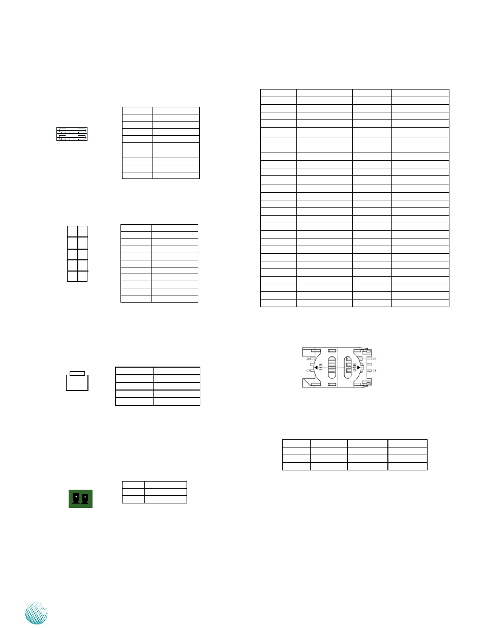
SIM Card Reader (CN9)
Pin NO.
signal
Pin NO.
signal
C1
UIM_PWR
C5
GNd
C2
UIM_RsT#
C6
UIM_VPP
C3
UIM_CLK
C7
UIM_dATA
1 2 3 4
5 6 7 8
Pin No.
Pin Name
1
UsB1_VCC5
2
UsB1N/3N
3
UsB1P/3P
4
GNd
5
UsB0_VCC5/
UsB2_VCC5
6
UsB0N/UsB2N
7
UsB0P/UsB2P
8
GNd
Pin No.
Pin Name
1
PWR_BTN_N
2
VCC5_sB
1
3
2
4
2 1
10
8
6
4
2
9
7
5
3
1
Pin No.
Pin Name
1
UsB4_VCC5
2
GNd
3
N/A
4
UsB5P
5
UsB4N
6
UsB5N
7
UsB4P
8
N/A
9
GNd
10
N/A
C1
C3
C5
C7