Pam8403h, Thermal information, Electrical characteristics – Diodes PAM8403H User Manual
Page 4
PAM8403H
Document number: DSxxxxx Rev. 1 - 0
4 of 11
November 2012
© Diodes Incorporated
PAM8403H
A Product Line of
Diodes Incorporated
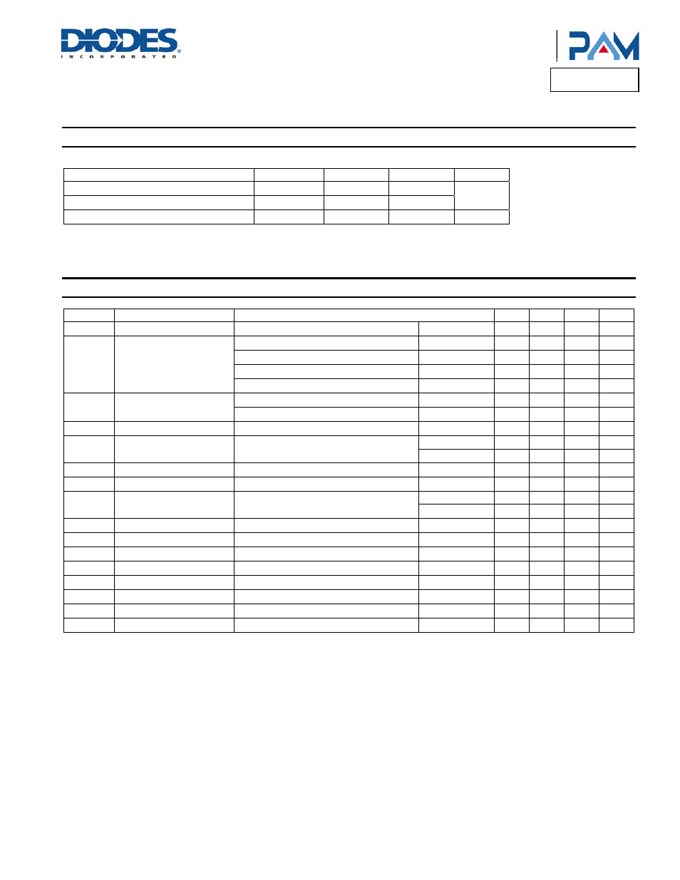
Thermal Information
Parameter Package
Symbol
Max
Unit
Thermal Resistance (Junction to Ambient)
SOP-16
θ
JA
110
°C/W
Thermal Resistance (Junction to Case)
SOP-16
θ
JC
23
Internal Power Dissipation (@ T
A
= +25°C)
SOP-16
P
D
90 mW
Note:
1. The maximun output current for SOT23-5 package is limited by internal power dissipation capacity as described in
Application Information here inafter.
Electrical Characteristics
(@T
A
= +25°C, V
DD
= 5V, Gain = 24dB, R
L
= 8
Ω, unless otherwise specified.)
Symbol Parameter
Test
Conditions
Min
Typ
Max
Units
V
IN
Supply Voltage
2.5
5.5
V
P
O
Output Power
THD+N = 10%,f = 1kHz , R
L
= 4
Ω
V
DD
= 5.0V
2.85 3.20
W
THD+N =1%, f = 1kHz, R
L
= 4
Ω
V
DD
= 5.0V
2.25 2.50
W
THD+N =10%,f = 1kHz, R
L
= 8
Ω
V
DD
= 5.0V
1.5 1.8 W
THD+N = 1%, f = 1kHz, R
L
= 8
Ω
V
DD
= 5.0V
1.2 1.4 W
THD+N
Total Harmonic Distortion
Plus Noise
V
DD
= 5.0V,P
O
= 0.5W, R
L
= 8
Ω
f = 1kHz
0.15
0.20
%
V
DD
= 5.0V, P
O
= 1W, R
L
= 4
Ω
f = 1kHz
0.15
0.20
%
G
V
Gain
23 24 25 dB
PSRR
Power Supply Ripple
Rejection
V
DD
= 5.0V, Inputs AC-grounded with
C
IN
= 0.47
μF
f = 100Hz
-59
-50
dB
f = 1kHz
-58
-50
dB
C
S
Crosstalk
V
DD
= 5V, P
O
= 0.5W, R
L
= 8
Ω, G
V
= 20dB
f = 1kHz
-95
-80
dB
SNR
Signal-to-Noise Ration
V
DD
= 5V, V
ORMS
= 1V,G
V
= 20dB
f = 1kHz
74 80 dB
V
N
Output Noise
V
DD
= 5V, Inputs AC-Grounded with
C
IN
= 0.47
μF
A-weighting
100
200
No A-weighting
150
300
µV
I
Q
Quiescent Current
V
DD
= 5.0V
No load
16
20
mA
I
MUTE
Muting Current
V
DD
= 5.0V
V
MUTE
= 0.3V
8
12
mA
I
SD
Shutdown Current
V
DD
= 2.5V to 5.5V
V
SD
= 0.3V
20
µA
V
OS
Output Offset Voltage
V
IN
= 0V, V
DD
= 5V
10 mV
V
IH
Enable Input High Voltage
V
DD
= 5.0V
1.5 V
V
IL
Enable Input LowVoltage
V
DD
= 5.0V
0.4
V
V
IH
MUTE Input High Voltage
V
DD
= 5.0V
1.5 V
V
IL
MUTE Input Low Voltage
V
DD
= 5.0V
0.4
V