Pam2312, Pin descriptions, Functional block diagram – Diodes PAM2312 User Manual
Page 2: Absolute maximum ratings
PAM2312
Document number: DSxxxxx Rev. 2 - 0
2 of 14
January 2013
© Diodes Incorporated
PAM2312
A Product Line of
Diodes Incorporated
Pin Descriptions
Pin
Name
TSOT25
Function
Pin Name
4 VIN
Chip main power supply pin.
2 GND
Ground
1 EN
Enable Control Input. Force this pin voltage above 1.5V, enables the chip, and below
0.3V shuts down the device.
5 VOUT/FB
VOUT: Output voltage feedback pin, an internal resistive divider divides the output
voltage down for comparison to the internal reference voltage.
FB: Feedback voltage to internal error amplifier, the threshold voltage is 0.6V.
3 SW
The drains of the internal main and synchronous power MOSFET.
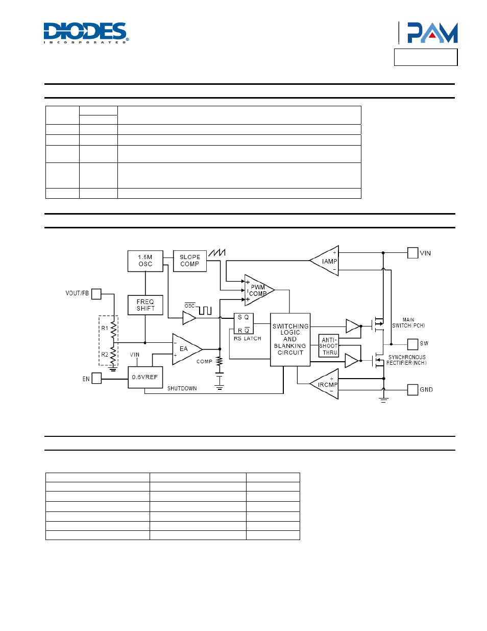
Functional Block Diagram
Absolute Maximum Ratings
(@T
A
= +25°C, unless otherwise specified.)
These are stress ratings only and functional operation is not implied. Exposure to absolute maximum ratings for prolonged time periods may
affect device reliability. All voltages are with respect to ground.
Parameter Rating
Unit
Inout Voltage
-0.3 to +6.0
V
EN, FB Pin Voltage
-0.3 to V
IN
V
SW Pin Voltage
-0.3 to (V
IN
+0.3)
V
Junction Temperature
150
°C
Storage Temperature Range
-65 to +150
°C
Soldering Temperature
300, 5sec
°C