Maximum ratings, Thermal characteristics, Electrical characteristics – Diodes DMN6070SSD User Manual
Page 2
DMN6070SSD
Document number: DS36342 Rev. 2 - 2
2 of 6
September 2013
© Diodes Incorporated
DMN6070SSD
NEW PROD
UC
T
ADVAN
CE I
N
F
O
RM
ATI
O
N
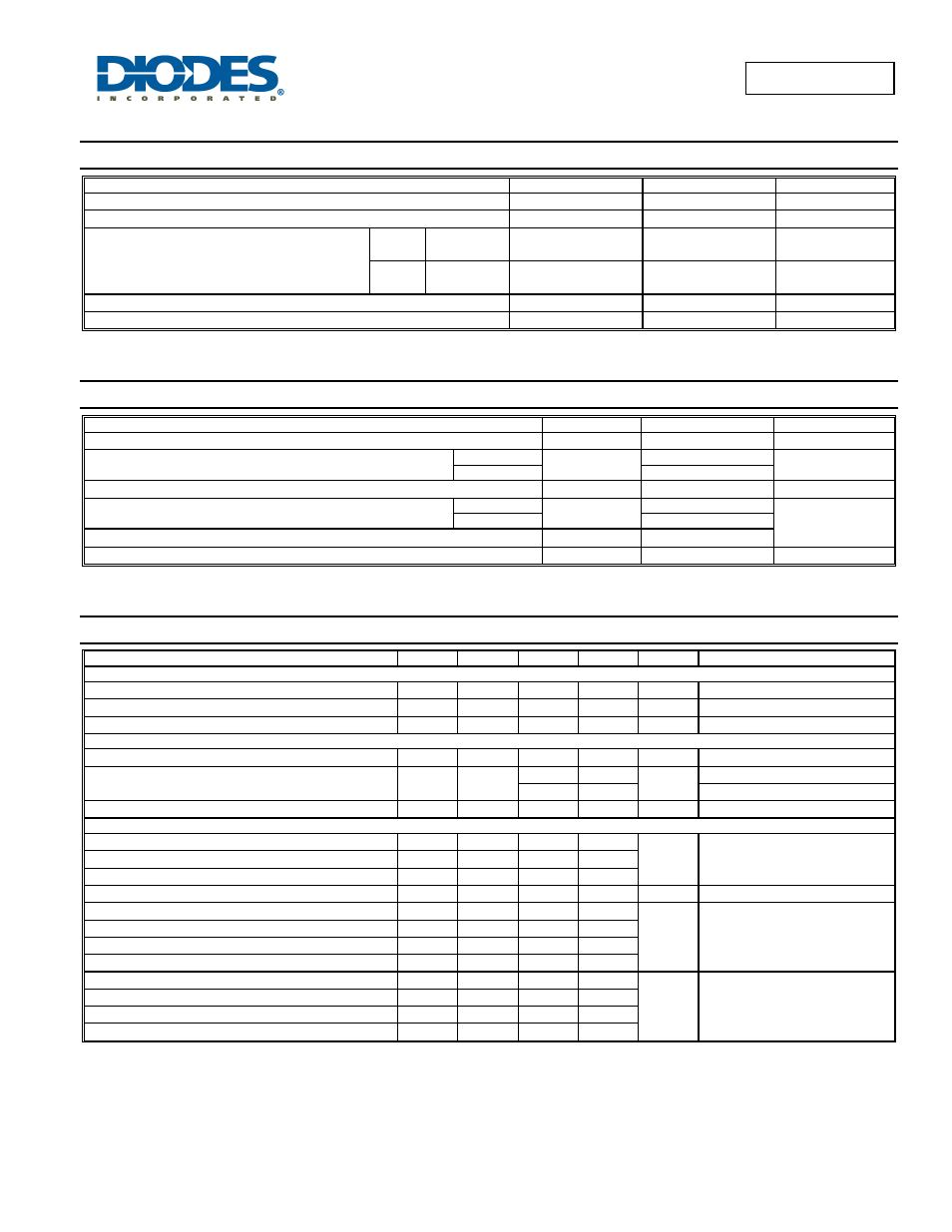
Maximum Ratings
(@T
A
= +25°C, unless otherwise specified.)
Characteristic Symbol
Value
Units
Drain-Source Voltage
V
DSS
60 V
Gate-Source Voltage
V
GSS
±20 V
Continuous Drain Current (Note 6) V
GS
= 10V
Steady
State
T
A
= +25°C
T
A
= +70°C
I
D
3.3
2.6
A
t<10s
T
A
= +25°C
T
A
= +70°C
I
D
4.1
3.4
A
Maximum Continuous Body Diode Forward Current (Note 5)
I
S
2.0 A
Pulsed Drain Current (10μs pulse, duty cycle = 1%)
I
DM
12 A
Thermal Characteristics
(@T
A
= +25°C, unless otherwise specified.)
Characteristic Symbol
Value
Units
Total Power Dissipation (Note 5)
P
D
1.2 W
Thermal Resistance, Junction to Ambient (Note 5)
Steady State
R
JA
104
°C/W
t<10s 61
Total Power Dissipation (Note 6)
P
D
1.5 W
Thermal Resistance, Junction to Ambient (Note 6)
Steady State
R
JA
83
°C/W
t<10s 50
Thermal Resistance, Junction to Case
R
JC
14.5
Operating and Storage Temperature Range
T
J,
T
STG
-55 to +150
°C
Electrical Characteristics
(@T
A
= +25°C, unless otherwise specified.)
Characteristic Symbol
Min
Typ
Max
Unit
Test
Condition
OFF CHARACTERISTICS (Note 7)
Drain-Source Breakdown Voltage
BV
DSS
60
V
I
D
= 250μA, V
GS
= 0V
Zero Gate Voltage Drain Current
I
DSS
1
μA
V
DS
= 60V, V
GS
= 0V
Gate-Source Leakage
I
GSS
100
nA
V
GS
=
16V, V
DS
= 0V
ON CHARACTERISTICS (Note 7)
Gate Threshold Voltage
V
GS(th)
1.0
3.0 V
I
D
= 250μA, V
DS
= V
GS
Static Drain-Source On-Resistance
R
DS (ON)
68
80
mΩ
V
GS
= 10V, I
D
= 12A
70 100
V
GS
= 4.5V, I
D
= 6A
Diode Forward Voltage
V
SD
0.75 1.1 V
I
S
= 12A, V
GS
= 0V
DYNAMIC CHARACTERISTICS (Note 8)
Input Capacitance
C
iss
588
pF
V
DS
= 30V, V
GS
= 0V
f= 1MHz
Output Capacitance
C
oss
26.5
Reverse Transfer Capacitance
C
rss
20
R
g
1.5
Ω
Vgs= 0V, Vds= 0V, f=1MHz,
Total Gate Charge (V
GS
= 4.5V)
Q
g
5.6
nC
V
DS
= 30V, I
D
= 3A
Total Gate Charge (V
GS
= 10V)
Q
g
12.3
Gate-Source Charge
Q
gs
1.7
Gate-Drain Charge
Q
gd
1.9
Turn-On Delay Time
t
D(on)
3.5
nS
V
DD
= 30V, V
GS
= 10V
R
L
50Ω, R
G
20Ω
Turn-On Rise Time
t
r
4.1
Turn-Off Delay Time
t
D(off)
35
Turn-Off Fall Time
t
f
11
Notes:
5. Device mounted on FR-4 substrate PC board, 2oz copper, with minimum recommended pad layout.
6. Device mounted on FR-4 substrate PC board, 2oz copper, with 1inch square copper plate.
7. Short duration pulse test used to minimize self-heating effect.
8. Guaranteed by design. Not subject to product testing.